J-FET
The J-FET is, like a MOSFET, a voltage controlled transistor. It differs from (most) MOSFETs that it will conduct the maximum amount of current with zero voltage at the gate, and this conduction is decreased when more (negative) voltage is applied to the gate. A J-FET has a very large gate impedance, so essentially no current passes the gate. Typically, the capacitance of the gate is low, so it is very useful when a high impedance input is needed.
The figure below gives the correlation between Vds and Id. The topmost, green line depics the correlation at Vg = 0V. At this point, the maximum current (Id = 2mA) is available.
This figure is calculated from the spice model. It doesn resembles pretty good the diagram as it is depicted in the actual datasheet for a 2SK30A-Y. In the original datasheet, the max Ids is larger, but this value depends a lot on the specific specimen: the range might be between 1.2mA and 3mA for a class Y transistor.
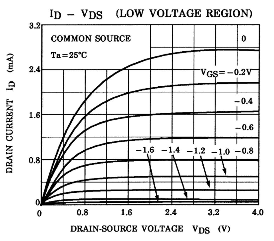
To act as a (linear) amplifier it is important that the gate is biased so that Vgs < 0V, but not to much, as this will turn off the transistor completely. The actual bias point should be such that the swing never goes above 0V. It’s also important that Vgs isn’t close to the “bottom” of this drawing, as in this area the linearity is less (the lines are much more closer together, which will mean that the bottom half of the signal will be amplified less than the top half).
It is also very important that the bias resistors are very large (in the order of 1G), so we don’t loose the high input impedance of the circuit.