Treble booster wiring
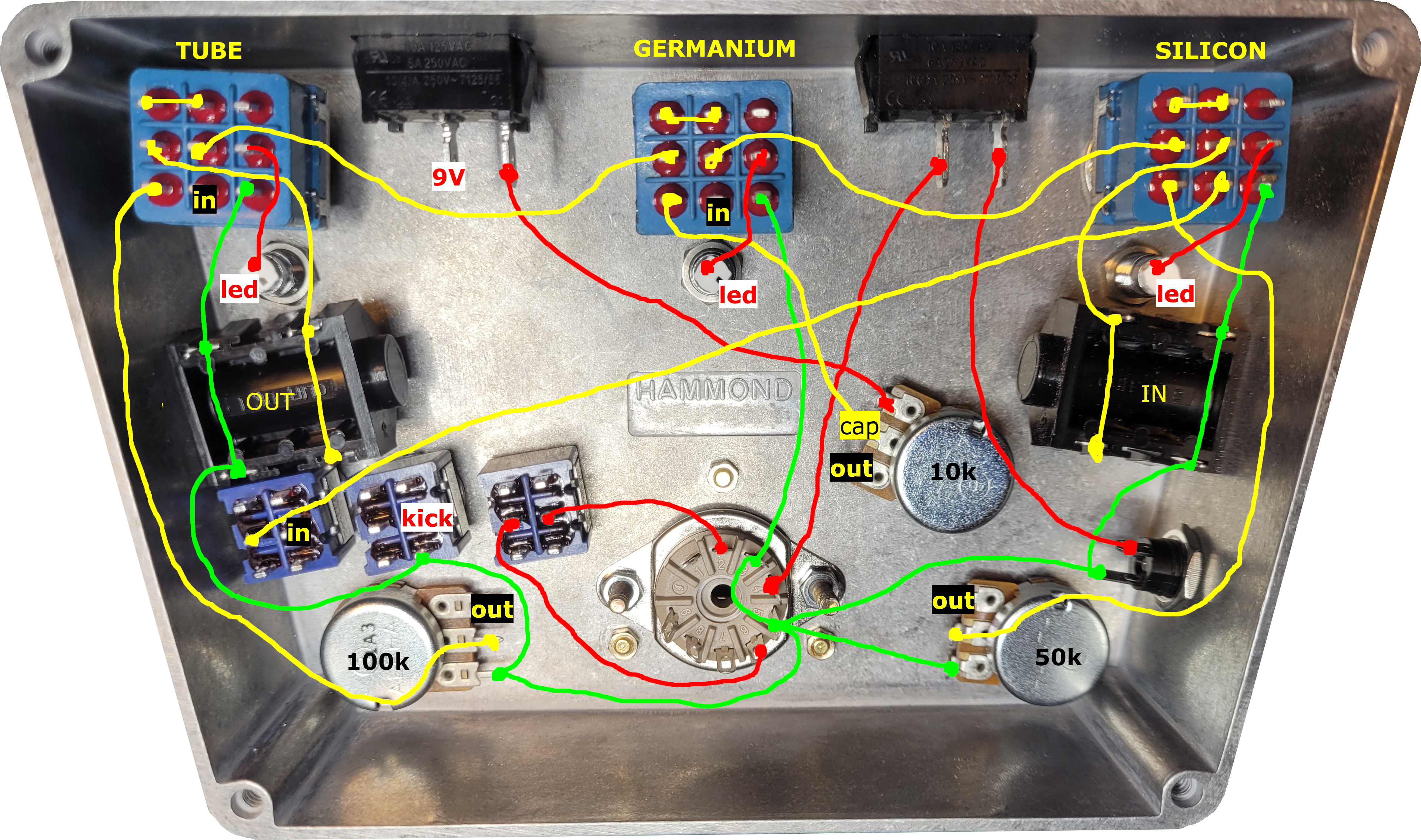
The depicted wiring is between elements in the top of the case, the following connections need to be made to the PCB:
The GREEN wires are all GND should be connected to the GND of the PCB. The YELLOW wires conduct the signal path from IN to OUT. The RED wires are switch connections and LED connections.
To be decided: the original Rangemaster en Treble booster had a shunt diode as reverse polarity protection. This is not yet included, but can be easily added between the legs of the power socket.
Every LED will have a 1kΩ resistor between the LED cathode and the footswitch. The LED anode will be connected directly to 12V.
| Nr | Name | Connection |
|---|---|---|
| - | led | LED Si booster |
| - | led | LED Ge booster |
| - | led | LED Tube booster |
| 1 | kick | Tube booster kick resistor switch |
| 2 | in | Input of Tube booster circuit |
| 3 | in | Input of Ge booster circuit |
| 4 | in | Input of Si booster circuit |
| 5 | out | Output of Tube booster circuit |
| 6 | out | Output of Ge booster circuit |
| 7 | out | Output of Si booster circuit |
| 8 | P1 | Pin 1 of Tube socket |
| 9 | P2 | Pin 2 of Tube socket |
| 10 | P6 | Pin 6 of Tube socket |
| 11 | P7 | Pin 7 of Tube socket |
| 12 | P8 | Pin 8 of Tube socket |
| 13 | GND | Ground (green wires) |
| 14 | V9 | 9V connection |
| 15 | V12 | Power socket |
The wires for these connections will be bundled into a dupon connector, so the connection between the PCB and the backplate is just one simple dupon connector.
The Capacitor selector switches (for the Si booster and the Tube booster) will have the capacitors soldered to them, that’s easier than on the PCB. R15 (120kΩ) will also be soldered directly to the switch. R15 should be soldered between the green wire (GND) and the yellow wire that is connected to the leftmost switch. Also notice the output capacitor C17 (10nF) that is connected between the 10kΩ pot and the footswitch.
Signal path
- Silicon
- Signal input through right jack socket;
- SI-footswitch: from there to the GE-footswitch, or the SI-circuit;
- Input Capacitor selector switch;
- Via the dupon connector [4] into the PCB SI-circuit;
- Via the dupon connector [7] out of the PCB SI-circuit into the 50k pot;
- From the pot back to the SI-footswitch
- Germanium
- Signal from the SI-footswitch
- GE-footswitch: from there to the TUBE-footswitch, or the GE-circuit;
- Via the dupon connector [3] into the PCB GE-circuit;
- Via the dupon connector [6] out of the PCB GE-circuit into the 10k pot;
- From the pot, through the output capacitor back to the GE-footswitch
- Tube
- Signal from the GE-footswitch
- TUBE-footswitch: from there to the output jack socket, or the TUBE-circuit;
- Via the dupon connector [2] into the PCB TUBE-circuit;
- Via the dupon connector [11] to P7 (grid);
- From P6 (anode) to the capacitor selector switch;
- From the capacitor selector switch to P2 (grid);
- From P1 (anode) via the dupon connector [8] back to the PCB TUBE-circuit;
- Via the dupon connector [5] out of the PCB TUBE-circuit into the 100k pot;
- From the pot back to the TUBE-footswitch
- Signal output through left jack socket.
The tube circuit needs a couple of more connections:
- Dupon connector [9] to P2 (grid);
- Dupon connector [10] to P6 (anode);
- Dupon connector [12] to P8 (cathode);
- Dupon connector [1] to kick switch.
Ground and power connections:
- Dupon connector [13] to GND power socket;
- Dupon connector [14] to the 9V output from the PCB;
- Dupon connector [15] to 12V power socket.
Dupon connectors
The picture below shows the final routing, with the dupon connectors (two 8-pin connectors, female). The table below gives the pinout:
| Pin | Connection |
|---|---|
| 1 | 9V (red wire) |
| 2 | in Tube |
| 3 | kick |
| 4 | in Silicon |
| 5 | out Tube |
| 6 | pin 1 tube socket |
| 7 | pin 7 tube socket |
| 8 | pin 8 tube socket |
| Pin | Connection |
|---|---|
| 1 | 12V (red wire) |
| 2 | in Germanium |
| 3 | pin 2 tube socket |
| 4 | ground |
| 5 | out Germanium |
| 6 | out Silicon |
| 7 | pin 6 tube socket |
High pitch noise problem
The boosters seem to experience a problem: a high pitch noise is emitted from the circuit, which I can’t explain.
- The situation doesn’t occur with the full bypass (all LED’s off);
- The situation doesn’t occur with the Tube booster with the kick enabled;
- The situation does occur with the Tube booster and the kick disabled;
- The situation does occur with the Silicon and Germanium transistors
- The volume of the pots will increase or decrease the amount of noise.
It seems some kind of oscillation within the circuit, probably the PCB. Maybe the input power isn’t as clean as one would like!
The story continues…
- Removed the three resistors that form the resistor divider to deliver 9V
- Tested a 7809 circuit on the breadboard, using the 9V output as input => Problem fixed
- Put the 7809 circuit onto the PCB => Problem reoccurs…
It seems that the layout of the PCB creates the oscillation. The probable cause is that the ground of the 9V and 12V parts is shared (and not in a star configuration). The solution was to add an extra 12V connection to the board, and changed the Germanium switch to another 12V switch for the 9V part (as the current option in which the switch basically was already implemented in the pot of the Germanium circuit). This worked. So no high pitch with only the tube circuit enabled or only the transistor circuits (Ge and Si). The high pitch is present when both circuits are enabled, but that can only be fixed by making a new PCB…